Introduction
The field of PCB manufacturing relies on a variety of technologies to produce high-quality circuit boards used in electronic devices. In this article, we'll explore some of the key technologies utilized by pcb manufacturer to fabricate PCBs efficiently and accurately.
PCB Design Software
- Computer-Aided Design (CAD): PCB manufacturers employ CAD software such as Altium Designer, Eagle, or KiCad for schematic capture and PCB layout design.
- Design for Manufacturing (DFM) Tools: DFM tools help identify potential manufacturing issues early in the design phase, optimizing the PCB layout for manufacturability and cost-effectiveness.
Fabrication Processes
- Etching: PCB manufacturers use chemical etching or mechanical milling processes to remove copper from the substrate according to the circuit pattern.
- Printing Methods: Advanced printing techniques such as inkjet printing or screen printing are employed for applying solder mask and legend onto the PCB surface.
- Drilling: High-speed precision drilling machines with automated tool changers are used to create holes for component mounting and vias.
Surface Finishing Techniques
- Hot Air Solder Leveling (HASL): HASL is a common surface finish method where molten solder is applied to the copper pads to facilitate component soldering.
- Electroless Nickel Immersion Gold (ENIG): ENIG provides excellent corrosion resistance and solderability, making it suitable for high-reliability applications such as aerospace and medical devices.
- Immersion Silver (ImAg): Immersion silver coating offers a flat surface finish and good solderability, ideal for fine-pitch components and high-frequency circuits.
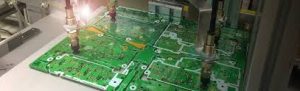
Assembly Processes
- Surface Mount Technology (SMT): SMT involves placing surface-mount components directly onto the PCB using pick-and-place machines, followed by reflow soldering in a controlled atmosphere.
- Through-Hole Assembly: Through-hole components are inserted into pre-drilled holes on the PCB and soldered manually or using wave soldering machines.
- Automated Optical Inspection (AOI): AOI systems utilize cameras and image processing algorithms to detect defects such as solder bridges, missing components, or misalignment in assembled PCBs.
Quality Control Measures
- Electrical Testing: PCB manufacturers conduct electrical tests such as continuity testing, insulation resistance testing, and functional testing to ensure the integrity and functionality of the assembled boards.
- X-ray Inspection: X-ray inspection is used to detect defects such as voids in solder joints, hidden solder bridges, or component misalignment, especially in complex or densely populated PCBs.
Conclusion
PCB manufacturers employ a wide range of technologies throughout the design, fabrication, assembly, and quality control processes to produce high-quality circuit boards that meet the stringent requirements of various industries. By leveraging these advanced technologies, manufacturers like pcb manufacturer can deliver reliable and cost-effective PCB solutions to their customers.